Browse categories
Explore
Fiverr Pro
English
$
USD
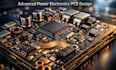
Power Electronics Multilayer PCB Design Studio
We are a UK-based Power Electronics & Multilayer PCB Design Studio led by Sarah.
We provide advanced schematic design and PCB layout for SMPS, DC-DC converters, inverters, BMS, motor drivers, high-current power supply systems, IoT, and embedded hardware.
What you get:
PERFECT FOR
FEW OF THE TOOLS WE USE;
DO YOU HAVE ANY QUESTION OR WANT TO DISCUSS MORE ABOUT YOUR PROJECT, JUST A MESSAGE TO SARAH'S_ SOLVES AND GET THE BEST OF BEST BY THE BEST TEAM

Do you design high current PCB layouts?
Yes. We specialize in high-current copper routing, thermal optimization, and EMI-aware layouts.
Can you design multilayer and controller impedance boards?
Yes. We handle 2–6+ layers with stack-up, differential pairs, and signal integrity.
What files will i reccive?
You get production-ready Gerber files, drill files, BOMs, and full documentation.
Which tools do you use?
KiCad, OrCAD, EasyEDA, following industry-standard workflows.
What is this perfect for?
Hardware startups, EV developers, industrial power systems, IoT and embedded system prototypes.
