Browse categories
Explore
Fiverr Pro
English
$
USD
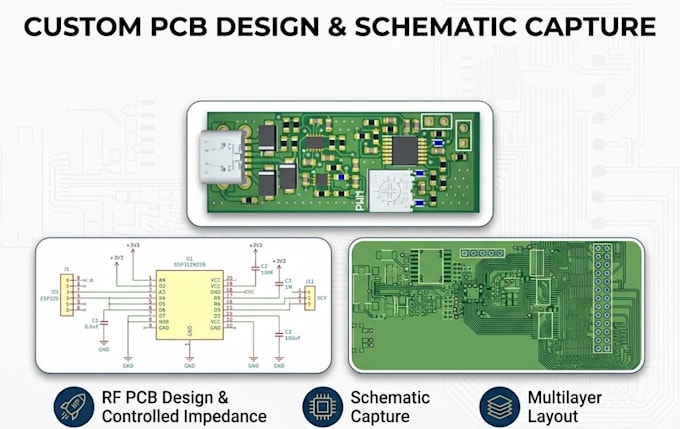
Custom PCB Design, RF Boards & Schematic Capture
Looking for a reliable designer to bring your circuit ideas to life? I deliver professional, production-ready PCB layouts and schematic capture tailored to your exact hardware needs.
What I Offer:
Note: High-speed interfaces (HDMI, PCIe, LTE/cellular) are outside the scope of this gig.
Every layout is DFM-optimised for quick manufacturing.
Please message me before placing an order to discuss your circuit details and project timeline!



What files do I need to provide to get started?
You need to provide your project requirements, block diagram, or hand-drawn/breadboard schematic, along with any specific component datasheets or board dimension constraints. If you already have a completed schematic, just send the design files.
What software do you use for PCB design?
I design primarily in Altium Designer, ensuring standard file compatibility and clean native project organisation. [EasyEDA and KiCAD support is also provided if needed]
Can you design boards with controlled impedance and RF layout?
Yes! I handle RF PCB routing, trace width/spacing calculations, and controlled impedance matching such as 50 ohms for WiFi and BLE, 90 ohms for USB, etc.
What deliverables will I receive upon completion?
You will get full production-ready manufacturing files: Gerber files, NC Drill files, Bill of Materials (BOM with component footprints/LCSC parts where applicable), Pick-and-Place (CPL) files, and 3D STEP/PDF view files.
What software do you use for SI and PI analysis?
I use CST Studio for such electromagnetic simulations to ensure accurate simulations.