Browse categories
Explore
Fiverr Pro
English
$
USD
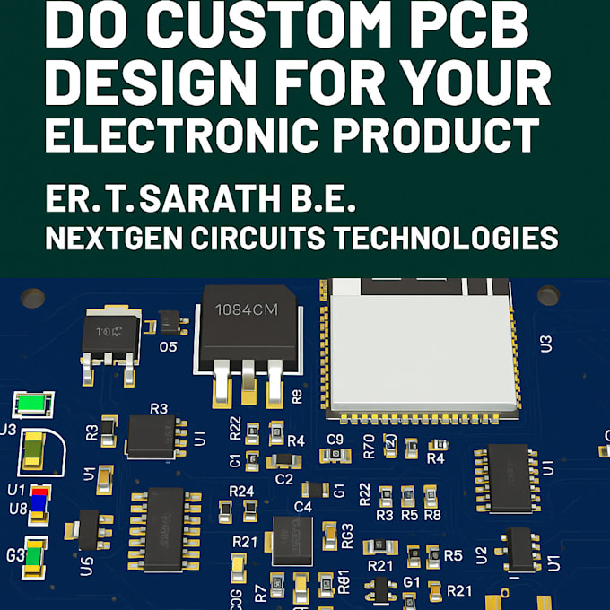
Welcome to NextGen Circuits Your Go-To PCB Design Expert!
Are you looking to bring your electronic product to life with a high-quality, optimized PCB layout?
Im Sarath T, an experienced PCB and embedded systems developer, and I specialize in designing custom PCBs for real-world applications.
My Services Include:
Tools I Use:
Deliverables:
Why Choose Me?
NDA Friendly & 100% Client Satisfaction Guaranteed!
Contact me before placing an order for a better understanding of your requirements.


What do I need to provide before starting?
Basic schematic (or hand sketch), functional requirement, preferred tools (if any), and desired board size.
Can you help me from idea to final PCB?
Yes! I can help from concept → schematic → PCB → Gerber + files for manufacturing.
Do you offer only 2-layer PCBs?
I support up to 11 layers. If you need more, please message me first.