Browse categories
Explore
Fiverr Pro
English
$
USD
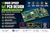
Professional PCB Design and Electronics Engineer
Are you looking for a professional high-speed IoT PCB design with proper EMI/EMC compliance and signal integrity optimization?
You are in the right place.
I specialize in designing reliable, manufacturing-ready high-speed PCBs for IoT, embedded systems, wireless communication, and industrial electronics.
Whether your project involves:
ESP32 / ESP8266 systems
WiFi & Bluetooth devices
RF and wireless communication
High-speed signal routing
USB, Ethernet, SPI, UART, CAN interfaces
Multi-layer PCB layouts
EMI/EMC optimization
Noise reduction techniques
Industrial IoT systems
I can help you design a stable and production-ready PCB.
Services Included
Professional schematic design
High-speed PCB layout
EMI/EMC-aware routing
Ground plane optimization
Differential pair routing
Controlled impedance routing
Power integrity optimization
Signal integrity analysis
Decoupling and filtering optimization
Gerber & manufacturing files
BOM & Pick and Place files
3D PCB rendering

Can you design multi-layer high-speed PCBs?
Yes, I can design up to 8-layer high-speed PCBs with optimized routing.
