Browse categories
Explore
Fiverr Pro
English
$
USD
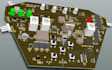
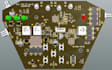
Expert RF And PCB Designer, Antenna, IoT, HDI, Multilayer PCB And RF Circuit
Hello, I'm a professional RF & PCB deslgner with over 5+ years of experience in deslgning high performance RF, WiFi, and Bluetooth circuits. I specialize in flexible PCB schematic deslgn, RF circuit optimization, and EMI/EMC compliance, ensuring your project meets the highest industry standards.
What I Offer:
Deliverables:
Why Choose Me:
Software I Use:
Lets turn your RF project into a high quality, ready to manufacture PCB.
NOTE: Kindly contact me first before placing an order to discuss your project requirement Thanks.
What types of RF PCB projects do you handle?
I design RF circuits, WiFi, Bluetooth, IoT devices, and wireless communication modules. From simple 2-layer PCBs to complex multi-layer high-frequency designs, I ensure full EMI/EMC compliance.
What files will I receive after the order?
You’ll get complete schematic and PCB layout files, Gerber files ready for manufacturing, BOM, and simulation/EMI optimization reports if required.
Can you optimize my design for EMI and EMC compliance?
Yes! I specialize in EMI/EMC optimization to reduce interference, improve signal integrity, and meet industry standards for high-performance RF circuits.
How long does it take to complete a project?
Most projects are completed within 5–7 days, depending on complexity. Rush delivery is available for urgent projects.
Do you provide revisions and support after delivery?
Absolutely! I include revisions depending on your package (1–unlimited), and I provide guidance to ensure your PCB is manufacturing-ready and fully functional.


