Browse categories
Explore
Fiverr Pro
English
$
USD
It's all about Quality Work and Fast Communication
Level 2
Has met high performance criteria and has a proven track record for meeting client expectations.
Is your PCB ready for manufacturing, or could hidden design errors lead to costly fabrication issues? I provide professional PCB design review and Design for Manufacturability (DFM) checks to help identify potential problems before you send your board for production.
Tools:
I will review your schematic, PCB layout, and manufacturing files to improve design quality and reduce avoidable production delays.
My services include:
Whether you have a 2-layer or multilayer PCB, an IoT device, or an RF or high-speed board, I focus on accuracy, manufacturability, and practical engineering solutions.
What makes my service valuable?
NOTE: Contact me before ordering.
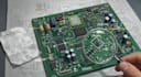
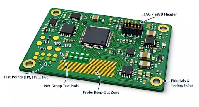
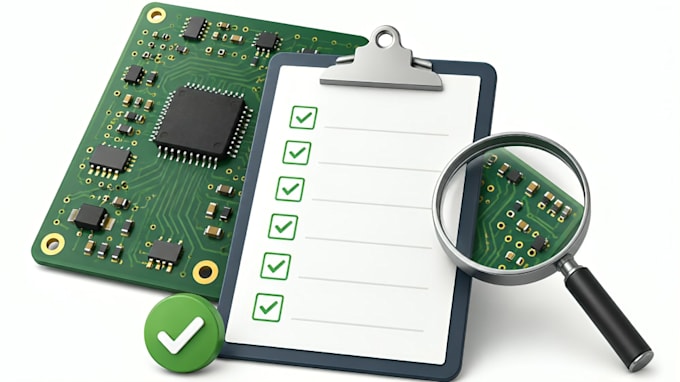
What is PCB Design for Manufacturability (DFM)?
DFM is the process of checking a PCB design for potential fabrication and assembly issues before production. It helps identify problems that could cause delays, extra costs, or manufacturing difficulties.
What files do you need to review my PCB?
Please provide your PCB layout and schematic files, preferably in the original design software format. Gerber files, drill files, BOM, component datasheets, and manufacturer specifications are also helpful.
What aspects of my PCB will you check?
I can inspect trace widths, clearances, vias, footprints, drill sizes, copper spacing, silkscreen, grounding, power routing, and other relevant manufacturing requirements.
Will you fix the problems found during the review?
Yes. Design corrections and optimization can be included depending on your project requirements. Please contact me to confirm the scope before ordering.
Can you review RF, high-speed, or power electronics PCBs?
Yes. I can review relevant layout considerations for RF, high-speed signals, and power electronics. Please provide the schematics, design constraints, and applicable specifications.
Can you guarantee my PCB will work perfectly after manufacturing?
A design review can help identify potential problems, but it cannot guarantee flawless manufacturing or circuit operation. Physical fabrication, assembly, and functional testing may still be necessary to verify the final board.