Browse categories
Explore
Fiverr Pro
English
$
USD
Electrical and Electronic Engineer, PCB design, Embedded firmware
With over 24 years in academia and industry, I have guided and worked alongside my students in designing PCBs for a wide range of electronic circuits as part of multiple university-level courses and projects. Many of my students have taken these skills forward and are already delivering PCB designs at a commercial level.
Now, I am bringing this extensive experience to the freelancing world to help you turn your ideas into reliable, production-ready PCBs.
Here's what you can expect:
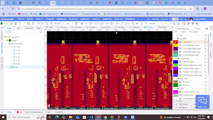
1. Schematic design and verification
2. Accurate footprint creation for components
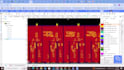
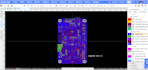
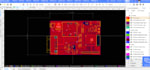
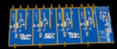
3. Professional PCB layout design (single, double, or multi-layer)
4. Design Rule Check (DRC) and Electrical Rule Check (ERC)
5. Generating Gerber files, BOM, drill files, pick & place files
6. 3D PCB model (STEP or VRML) for enclosure fitting
7. Ready-to-manufacture files with full support
Whether you need a simple prototype or a complex multi-layer PCB, I ensure quality, clear communication, and delivery you can trust.


Do you provide the schematic too?
Yes, I can design both the schematic and PCB layout as needed.
Can you help me with component selection?
Yes, I can suggest suitable components and provide a BOM.
Can you sign an NDA?
Absolutely! Confidentiality is guaranteed.
Do you offer revisions?
Yes, revisions are included to ensure you get exactly what you need.