Browse categories
Explore
Fiverr Pro
English
$
USD
Microcontroller Engineer Intern PCB Designer
Are you looking for a professional PCB designer to turn your circuit ideas, block diagrams, or breadboard prototypes into a high-quality, production-ready PCB layout? You are in the right place!
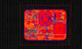
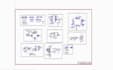
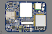
I specialize in Schematic Capture and PCB Layout Design using Easy-EDA, delivering clean, reliable, and noise-free circuit board designs ready for manufacturing at factories like JLCPCB, PCBWay, or Seeed Studio.
What I Offer:
Deliverables You Will Get:
Why Work With Me?
Note: Please contact me before placing an order to discuss your project requirements, component availability, and board specifications!


File format:
Gerber
•
STEP
•
3DS
•
Software:
EasyEDA
•
KiCad
•
Matlab
•
Simulink
•
Arduino
Interface:
UART
•
USB
•
SPI
•
I2C
•
Wi-Fi
•
BLE
•
BT
•
GSM/GPRS
What software do you use for PCB design?
I primarily design schematics and PCB layouts using Easy-EDA. I can deliver complete production-ready native Easy-EDA source files along with all standard manufacturing outputs.
What deliverables will I receive when the order is completed?
You will receive full manufacturing files including Gerber files (RS-274X), NC Drill files, Bill of Materials (BOM) with LCSC part numbers, a 3D STEP model for enclosure design, PDF schematics, and the source design files.
What information do I need to provide to start the project?
To get started, please provide your basic project requirements or objectives, a list of key components (like ESP32, sensors, displays), a block diagram or hand-drawn sketch if possible, and any specific PCB dimension or enclosure constraints you have.
Can you design multi-layer PCBs and wireless/IoT circuits?
Yes! I have extensive experience routing 2-layer and multi-layer boards involving wireless modules (ESP32, 4G/LTE, GPS), power management circuits, and sensor interfaces (I2C, SPI, UART)
Will the Gerber files be ready for PCB fabrication factories like JLCPCB?
Absolutely! All generated Gerber, Drill, and BOM files strictly adhere to standard Design For Manufacturing (DFM) rules and are 100% ready for fabrication at JLCPCB, PCBWay, or Seeed Studio
Do you provide 3D enclosure-compatible files for my PCB?
Yes! Every PCB design includes a 3D STEP (.step) or OBJ file model. This allows you or your mechanical designer to easily import the circuit board into CAD tools like Fusion 360 or SolidWorks to design a perfectly fitted 3D-printed or custom enclosure.
What if the PCB manufacturing factory finds an error during their Design Rule Check (DRC)?
All designs are pre-checked for manufacturing compliance before delivery. However, if your chosen PCB factory (e.g., JLCPCB, PCBWay) raises any technical queries or DRC issues, I will update and modify the design files free of charge to ensure successful production.


