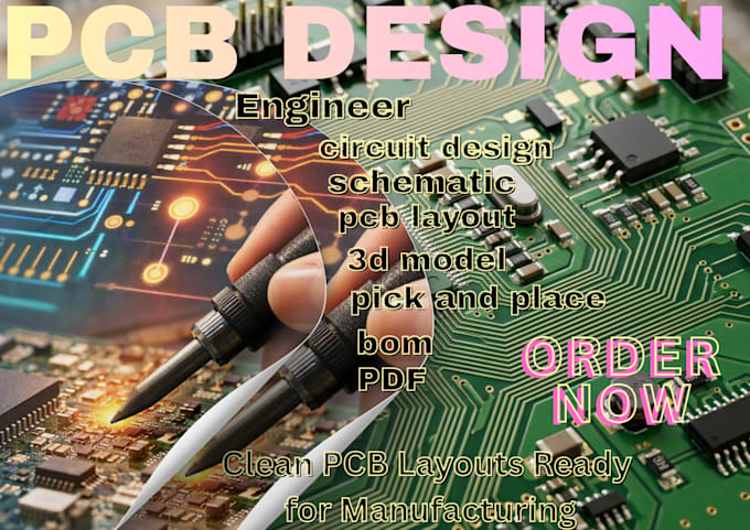
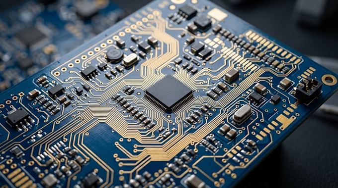
I will design professional pcb layout for manufacturing with clean routing and circuit


About this gig
I will design manufacturingready PCB layouts tailored to your project needs, using industrystandard tools such as Altium Designer, KiCad, Eagle, and OrCAD. Whether you need a quick prototype or a highspeed, multilayer board, I deliver clean routing, optimized stackups, and files ready for fabrication.
Packages
- Simple PCB Layout
- Perfect for hobby projects or prototypes. Includes 12 layer boards, basic routing, schematic capture, and Gerber files for fabrication.
- Complex PCB Layout
- Designed for professional applications. Includes 46 layer boards, mixed signal design, power distribution, BOM preparation, and Gerber/Drill files.
- Advanced PCB Layout
- Highend engineering for demanding projects. Includes highspeed design with impedance control, RF/microwave circuits, thermal management, and full stackup documentation with assembly drawings.
Deliverables
- Schematic & PCB layout files
- Gerber/Drill files ready for manufacturing
- Bill of Materials (BOM)
- Assembly drawings (for advanced package)
Why Choose Me
- Expertise in EDA tools (Altium, KiCad, Eagle, OrCAD)
- Focus on signal integrity, manufacturability, and reliability
- Clear communication and ontime delivery
hit up before placing your order
Get to know mark shelton
PCB Layout Engineer
- FromUnited States
- Member sinceAug 2026
- Avg. response time10 hours
Languages
English, Spanish, French
FAQ
What tools do you use?
I work with industry‑standard EDA software such as Altium Designer, KiCad, Eagle, and OrCAD, depending on client preference and project requirements.
What files will I receive?
You will receive schematic files, PCB layout files, Gerber/Drill files, and a Bill of Materials (BOM). For advanced packages, I also provide stackup documentation and assembly drawings.
Do you provide manufacturing support?
Absolutely. My layouts are manufacturing‑ready, and I can guide you through the fabrication process, including choosing PCB manufacturers.