Browse categories
English
$
USD
Connect to your AI
PCB Design and Electronics Engineering
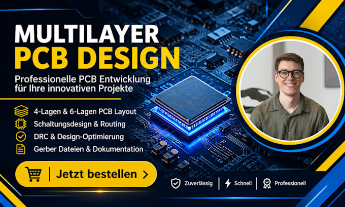
Need a Reliable Multilayer PCB Design for Your Next Electronics Project? Transform your electronic concepts into professionally structured multilayer PCB designs. I provide custom PCB layout, component placement, routing and layer stackup development tailored to your project requirements. Whether you need a 4-layer or more complex PCB, I focus on organized routing, appropriate de-sign-rule checks, signal integrity considerations and manufacturing-ready documentation using Altium Designer.
What My Buyers Will Get:
END RESULT:
CONTACT ME NOW.
Do you design 4-layer and multilayer PCBs?
Yes, I offer 4-layer and more complex multilayer PCB layouts based on your project specifications.
What information do you need to start my PCB design project?
I need your circuit schematic, component list, datasheets, board dimensions and specific design requirements.
Which software do you use for PCB design?
I primarily use Altium Designer for professional PCB schematic development, component placement and board layout.
Will I receive Gerber files for manufacturing?
Yes, I provide Gerber files, drill files and other agreed manufacturing documentation.
Can you redesign or improve an existing PCB layout?
Yes, I can review, modify and optimize existing PCB layouts according to your technical requirements.
Will I receive the editable PCB source files?
Yes, I provide the agreed editable Altium project files so you can review and make future modifications.
