Browse categories
Explore
Fiverr Pro
English
$
USD
HELLO
Expert PCB design production-ready schematics and layouts using top tools.
I deliver clean, reliable designs for IoT, embedded systems, power, analog/digital, sensors, and more optimized for performance and manufacturing.
Delivered package:
Tools: Altium Designer & KiCad (EasyEDA option)
Unlimited minor revisions, progress updates, and designs ready for JLCPCB, PCBWay, etc. Strong emphasis on signal/power integrity and EMC basics.
Share your project details (functional needs, constraints, references) I'll reply fast with quote and timeline. Let's build it right!
What info do I need to provide?
Project description, block diagram, specs (size, power, interfaces), key components, or references.
Which software do you use?
Altium Designer or KiCad primarily; EasyEDA also available.
Revisions included?
Yes — unlimited minor revisions until you're satisfied (scope unchanged).
Are files ready for production?
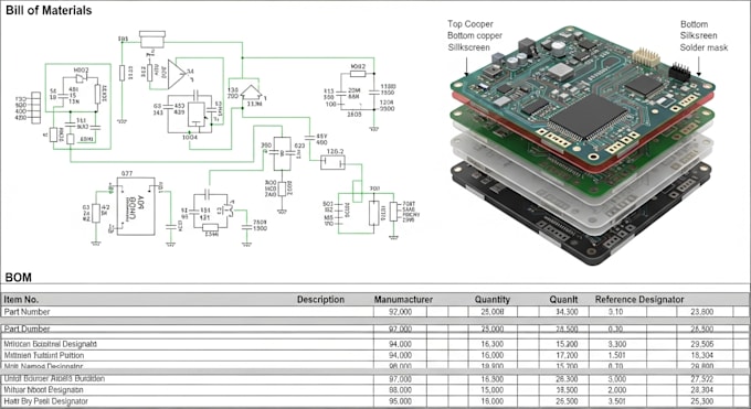
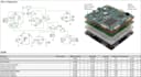
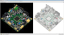
Yes — full Gerber set, drill, BOM, pick & place, DFM-optimized.
Can you start from just an idea?
Yes — I can develop the schematic from your description.
NDA available?
Yes, standard NDA signed gladly.
Delivery time?
3–5 days simple boards; 7–12 days complex/multilayer. Rush possible.