Browse categories
Explore
Fiverr Pro
English
$
USD
Turning ideas into reliable, production ready electronics
Welcome, clean design and reliable result
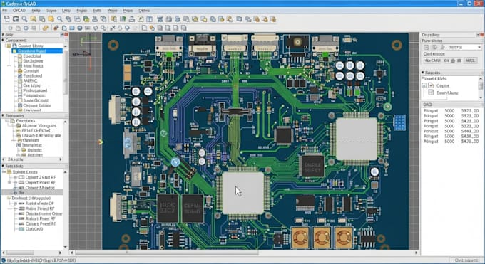
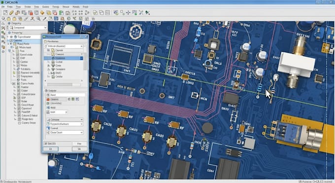
I'm a PCB design engineer with over 4 years of experience specializing in high speed RF circuits. I have designed RF PCBs operating at frequencies from 100MHz up to 21GHz, powering devices like smartphones, smart TVs, and wireless networks.
My expertise includes:
If you're planning to launch an RF product or need PCB verification on a VNA, I'm here to assist you. You can also hire me for testing and validation by sending your PCB.
Software I Use:
Feel free to message me to discuss your project I'm ready to bring your RF design ideas to life!

What information do you need to start an RF PCB design?
I need your frequency range, schematic (if available), board size, stack-up requirements, and target application.
Can you design high-frequency RF PCBs above 1 GHz?
Yes, I design RF PCBs from 100 MHz up to 21 GHz with proper impedance control and RF best practices.
Do you provide manufacturing and testing support?
Yes, I deliver fabrication-ready files and can also assist with VNA-based RF verification if required.