Browse categories
Explore
Fiverr Pro
English
$
USD
Expert PCB Design, Fast!
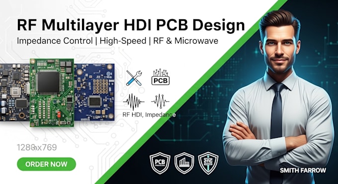
I will design a high-performance RF multilayer HDI PCB with precise impedance control using Altium Designer.
With strong expertise in RF and high-speed digital PCB design, I ensure your board meets strict signal integrity, power integrity, and manufacturability standards. Whether its a complex HDI stack-up or controlled impedance routing, I deliver production-ready designs optimized for performance and reliability.
What I offer:
Why choose me:
Lets turn your schematic into a high-quality, production-ready PCB that performs flawlessly at high frequencies.


What information do you need to start the PCB design?
I need your schematic, component datasheets, board size, layer requirements, stack-up details (if available), and any impedance or RF specifications.