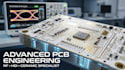
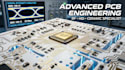
I specialize in High-Complexity PCB Engineering, focusing on RF, HDI, and Ceramic substrate designs. Whether you are working on a 5G communication module, a high-density mobile device, or a high-power industrial converter, I provide the precision layout necessary for signal integrity and thermal stability.
What I Offer:
- Layer Stack-up Design: Precise impedance-controlled stack-ups for high-speed signals.
- Comprehensive Gerber Package: RS-274X or X2 formats, including NC Drill and Pick-and-Place data.
- BOM Management: Detailed Bill of Materials with supplier links (DigiKey/Mouser) and lifecycle status.
- Assembly Drawings: Clear 2D/3D documentation for your fabrication house.
- Native Source Files: Full project files in Altium, KiCad, or EasyEDA for your future use.
Why Choose Me:
- Precision Engineering: I prioritize signal integrity and thermal management to prevent hardware failure.
- Global Standards: Designs are compliant with IPC-2221 and IPC-2222 standards.
- Confidentiality: I treat your IP with the highest security; NDAs are welcome.
Let's discuss your project constraints and build a high-performance solution tailored to your needs. Message me today to get started!