Browse categories
Explore
Fiverr Pro
English
$
USD
Welcome to my professional Schematic-to-PCB layout service!
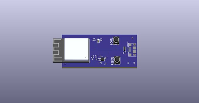
Need to transform your electronic circuit into a high-quality, production-ready Printed Circuit Board (PCB)? As an experienced Electronics Engineer, I will meticulously convert your schematics into optimized, reliable, and manufacturing-ready PCB layouts.
What I Offer:
- 1, 2, or Multi-layer PCB Layout design.
- Strict adherence to Design Rule Checks (DRC) & DFM guidelines.
- Signal & Power integrity optimization (including ESD protection & RF layout).
Deliverables You Will Receive:
- Gerber files (RS-274X) & NC Drill files (Ready for JLCPCB, PCBWay, etc.).
- Bill of Materials (BOM) with precise component footprints and MPNs.
...etc
Supported Software: KiCad
From compact IoT nodes (like ESP32/STM32) to complex multi-layer boards, I ensure your hardware is engineered for success.
Please contact me before placing an order to discuss your project requirements!


Specialization:
Circuit design
•
Schematics
•
Layout
•
Gerber
File format:
Gerber
•
STEP
•
SCH
•
Software:
KiCad
Interface:
UART
•
USB
•
SPI
•
I2C
•
Wi-Fi
•
BT
What files do I need to provide to start the project?
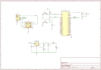
You need to provide your completed schematic diagram (as a project file from KiCad, or as a clean PDF/image). Please also share any specific requirements like board dimensions, mounting hole locations, or maximum enclosure height if available.
Will the final PCB files be ready for direct manufacturing?
Yes, absolutely! I generate standard Gerber files (RS-274X) and NC Drill files that are 100% compatible with all major PCB manufacturers worldwide, such as JLCPCB, PCBWay, and OshPark.
Do you provide the native source files of the design?
Yes, the native editable project files (KiCad) are included in all design packages at no extra cost, so you retain full ownership of your hardware design.