I will design custom pcb layouts and electronic schematics

India

I speak Telugu, English, Sanskrit, Japanese, Chinese

Engineer,trader,stocks manager

lI'm an interdisciplinary engineer specialising in electronics, PCB design, embedded systems, software development, AI/ML, DSP, RF engineering, FPGA and scientific computing. I also work with cybersec...
About this Gig

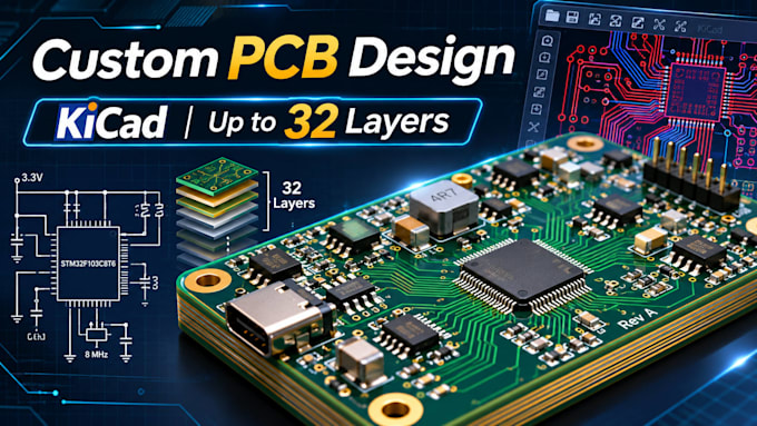
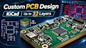
Need a reliable PCB design for your electronics project? I provide professional electronic schematic design and custom PCB layout services using KiCad.

My services include:

  • Custom analog and digital circuit design
  • Electronic schematic capture
  • Single-layer, double-layer and multilayer PCB layouts
  • Advanced multilayer PCB designs (up to 32 layers, subject to project requirements)
  • Component selection and BOM preparation
  • PCB placement, routing and design rule checks (DRC)
  • 3D PCB visualization and mechanical integration
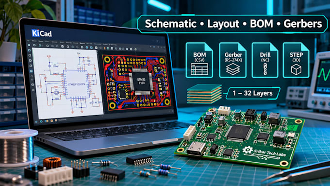
  • Gerber, drill and fabrication-ready file generation
  • Editable KiCad project files

I focus on organised layouts, practical engineering considerations and clear documentation.

Whether you're a hobbyist, student, startup, researcher or business, I can help turn your circuit concept into a manufacturable PCB design.

Deliverables: KiCad source files, schematic PDFs, BOM, Gerber files and other agreed outputs.

Please contact me before ordering for complex, high-speed, RF, high-voltage or advanced multilayer projects so we can discuss the specifications and requirements and even embedded work will be done if any thing related .

Let's bring your electronics ideas to life!
Specialization:

Circuit design

•

Schematics

•

Layout

•

Footprint

File format:

Gerber

•

STEP

•

BRD

•

SCH

•

PDF

Software:

Cadence OrCAD

•

KiCad

•

LTspice

•

Matlab

•

NI Multisim

•

Powersim

Interface:

HDMI

•

MIPI DSI/CSI

•

I2S

•

TDM

•

UART

•

USB

•

SPI

•

I2C

•

PCIe

•

Wi-Fi

•

BLE

•

BT