Browse categories
Explore
Fiverr Pro
English
$
USD
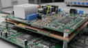
When you are pushing 20, 50, or 100 amps through a board, theoretical math is not enough. Most designers just think about connections, but high current is really about plumbing and thermodynamics. If the traces are too thin, the board acts like a fuse. If the thermal relief is wrong, you will never be able to solder the components.
I focus on path resistance, thermal dissipation, and making sure your connectors wont literally lift off the board under stress.
Service Included:
How it works:
1. You send me your schematic and current requirements
2. I calculate trace widths and thermal needs
3. I layout the board and optimize the power paths
4. You get the full production files and a design summary
Send over your schematic and let me check your current specs.