Browse categories
Explore
Fiverr Pro
English
$
USD
Top Tier Electronic Hardware and Firmware Engineer PCB Embedded RF Design
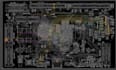
I will design high-speed, high-density HDI PCBs for complex electronics, including wearable SoC evaluation boards. My work covers BGA routing (0.35mm pitch), multi-layer PCB layout, schematic creation, BOM preparation, 3D modeling, and fabrication-ready files.
Whether you need a 12-layer HDI PCB with advanced interfaces like 4G, NFC, WLAN, or MIPI CSI, I provide precise, reliable, and optimized designs using Altium Designer.
Youll receive professional hardware engineering, accurate layouts, and ready-to-manufacture files for your high-performance electronics projects.


File format:
Gerber
•
STEP
•
SCH
•
•
ODB
Software:
Altium Designer
•
Eagle CAD
•
EasyEDA
•
KiCad
•
Matlab
Interface:
HDMI
•
I2S
•
UART
•
USB
•
SPI
•
I2C
•
Wi-Fi


