Browse categories
Explore
Fiverr Pro
English
$
USD
Indonesia
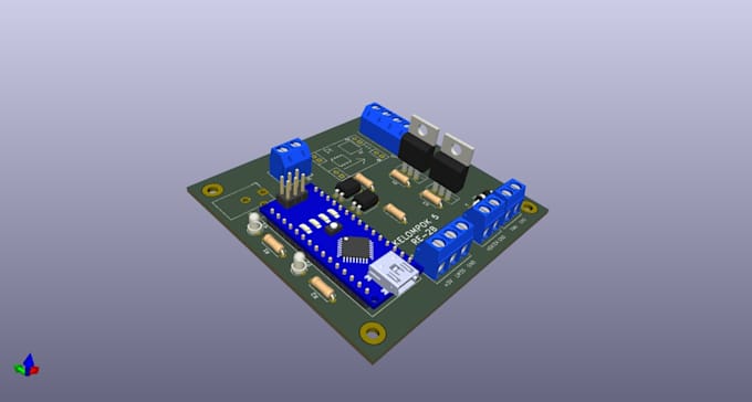
I Will Create Professional PCB Layout from Your Schematic
Do you need a clean, reliable, and manufacturing-ready PCB design?
I'm here to help turn your schematic or idea into a professional PCB layout ready for fabrication.
I specialize in custom PCB design for prototypes, educational projects, and microcontroller-based boards. Every PCB is designed with attention to clarity, reliability, and manufacturability.
What I offer:
Suitable for:
Why choose me:
Feel free to message me before ordering to discuss your project requirements.


Specialization:
Circuit design
•
Schematics
•
Layout
•
Footprint
•
Gerber
File format:
Gerber
•
STEP
•
SCH
•
Software:
Eagle CAD
•
EasyEDA
•
KiCad
•
Proteus
Interface:
UART
•
USB
•
SPI
•
I2C
•
Wi-Fi
What do I need to provide to start the project?
You can provide a schematic (PDF, image, or CAD file). If you don’t have one, please message me first to discuss your requirements.
Will I receive Gerber files?
Yes. All packages include manufacturing-ready PCB files, including Gerber files, ready to be sent to PCB manufacturers.
Do you provide component sourcing or PCB fabrication?
No. I provide PCB design services only. PCB manufacturing and component sourcing are handled by the client.
Can you review or fix an existing PCB design?
Yes. I can review or modify existing PCB layouts. Please contact me before ordering to discuss the scope.