Browse categories
Explore
Fiverr Pro
English
$
USD
HELLO AND WELCOME!!!
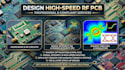
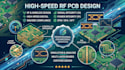
I will design a high-speed RF PCB optimized for EMI/EMC compliance, signal integrity, and manufacturability (DFM). If you are developing advanced electronics, IoT devices, communication hardware, or embedded systems, I will transform your schematic or concept into a reliable, production-ready PCB.
High-speed and RF boards require careful stack-up planning, controlled impedance routing, noise reduction, and proper grounding. I focus on creating layouts that perform reliably in real-world environments and pass manufacturing and testing smoothly.
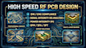
What I offer
Why choose me
Lets build a high performance PCB ready for real world production.
Which software do you use?
Altium, KiCad, OrCAD, and EasyEDA.
Can you work from concept only?
Yes, I can start from idea or schematic.
Will the PCB be ready for manufacturing?
Yes, files will be production-ready.
Do you design multilayer boards?
Yes, including high-speed and RF boards.
Can you fix EMI or signal integrity issues?
Yes, I can review and improve existing designs.


