Browse categories
Explore
Fiverr Pro
English
$
USD
Turning Innovative Ideas Into High Performance PCB Solutions
Hello there!!
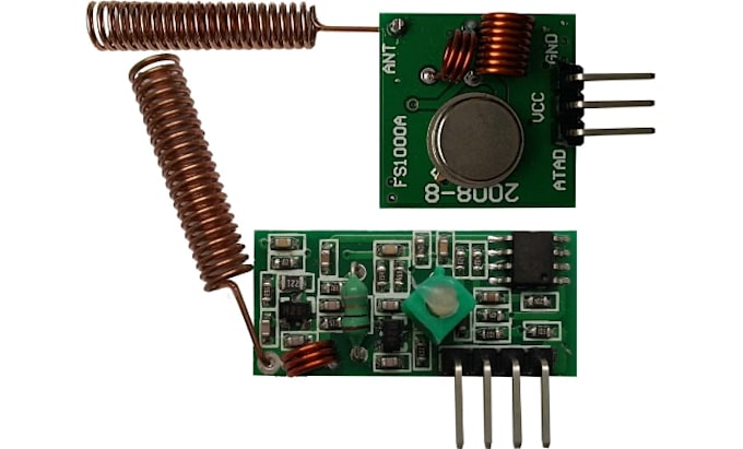
Are you facing signal loss, interference, poor wireless range, or unstable communication in your electronic product? I design reliable RF and high-speed PCB solutions with optimized routing, impedance control, and superior signal performance.
From IoT communication devices to advanced wireless hardware, I help startups, engineers, and companies develop production-ready RF electronic systems.
WHAT I OFFER
BENEFITS
Manufacturing ready Files
Quick delivery
Fast reponse
Friendly communication
Need a professional RF, wireless, or high-speed PCB for your next product?
Contact me today lets transform your idea into a reliable high-performance electronic solution.


Can you design custom RF and wireless communication PCBs?
Yes, I design custom WiFi, Bluetooth, LoRa, GSM, GPS, and other wireless communication PCBs based on your project requirements.
Do you optimize RF PCB layouts for signal integrity?
Yes, I focus on impedance matching, proper grounding, routing optimization, and EMI/EMC considerations for reliable RF performance.
Which files will I receive after project completion?
You will receive Gerber files, PCB layout, schematic, BOM, and other manufacturing documents