Browse categories
Explore
Fiverr Pro
English
$
USD
A poorly routed PCB introduces ground loops, cross-talk, high-frequency noise, and unexpected signal degradation. In high-end audio and precision hardware, bad board layout ruins an otherwise great circuit design.
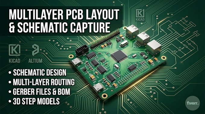
I specialize in engineering multi-layer PCB layouts and schematic capture using KiCad and Altium Designer. Whether you are building an analog audio preamplifier, a digital signal processor (DSP) module, a custom synthesizer, or a microcontroller-based controller, I route your circuits to strict hardware design standards.
What I Deliver:
Accurate Schematic Capture: Professional component symbol generation, clean multi-sheet schematics, and organized net structures.
High-Integrity PCB Layout: Optimized 2-layer to multi-layer routing with dedicated ground planes, controlled impedance traces, and strategic decoupling.
Complete Manufacturing Package: Gerber RS-274X/X2 files, NC Drill files, IPC-D-356 netlists, and assembly drawings.
SMT Assembly Ready: Formatted Bill of Materials (BOM) with part numbers (LCSC, DigiKey, Mouser) and Centroid/CPL pick-and-place files.
3D CAD Integration: 3D STEP models for exact mechanical enclosure alignment and front panel clearance