Browse categories
Explore
Fiverr Pro
English
$
USD
Embedded Systems Engineer, PCB Design and Firmware Developer
NOTE: Free consultation before you order. Send me your idea, schematic, existing PCB, or requirements, and I will review them and suggest the best approach.
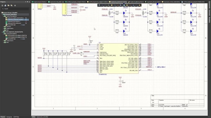
I help turn electronic ideas into reliable, production-ready PCBs that are ready for prototyping and manufacturing.
With 6+ years of experience in PCB design, schematic design, PCB layout, and embedded hardware, I work on IoT devices, embedded systems, industrial electronics, power electronics, and custom products.
WHAT YOU GET
TOOLS
WHY WORK WITH ME
Message me before ordering so I can review your project, confirm the scope, and recommend the best way forward.


What do you need to start my PCB design project?
I typically need your project requirements, circuit idea or block diagram, preferred components (if any), and specifications like size, layers, or constraints. Even a rough idea is enough to get started.
Which software and tools do you use?
I use industry standard tools like Altium Designer, EasyEDA and KiCad for PCB design, ensuring high quality, production ready outputs.
Do your files work directly with PCB manufacturers?
Yes. I deliver Gerber files, BOM, and CPL formatted for direct submission to assembly houses including JLCPCB, PCBWay, and others. DFM rules are applied throughout so your board goes straight to production.
Can you design PCBs for wireless IoT devices?
Yes. I have designed PCBs for ESP32, Nordic nRF, and other wireless modules with antenna placement, RF keep out zones, and EMI aware routing.
Can you help beyond PCB design (firmware, IoT, prototyping)?
Absolutely. At KernelCrew, we provide end-to-end solutions, from PCB design and firmware development to IoT integration and working prototypes.
What if I need support after the project is completed?
Yes, I provide post project support. If you need help after delivery whether it's minor changes, guidance, or troubleshooting. I’m available to assist. Long term support or additional work can also be arranged if needed.
What is your turnaround time?
A: Single and double layer boards are delivered in 2 to 3 days. 4 layer boards take 5 to 7 days. Complex multilayer boards take 10 to 12 days. I confirm the exact timeline before starting.