Browse categories
Explore
Fiverr Pro
English
$
USD
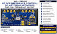
I'm a dedicated PCB engineer with 8 years experience in RF PCB design, high frequency circuits, impedance control and RF matching networks. I design reliable RF and high-speed PCB layouts with focus on signal integrity, controlled impedance routing and proper stack-up planning.
I provide PCB that reduce noise, improve signal flow and ensure stable RF performance. every design is carefully handled with attention to layout, spacing, grounding and frequency behavior for clean and efficient results.
What i offer:
What you will get:
Process:
Software used:
Send your project details and let's build a high-performance RF PCB.

What do you need to start my RF PCB project?
I need your schematic, requirements, operating frequency, and any size constraints.
Can you design impedance-controlled RF PCBs?
Yes, I ensure proper impedance control based on stack-up and trace calculations.
Do you provide manufacturing files?
Yes, I deliver Gerber files, drill files, and all files needed for fabrication.
Which software do you use?
I use tools like Altium Designer, KiCad, and RF simulation tools when required.
