Browse categories
Explore
Fiverr Pro
English
$
USD
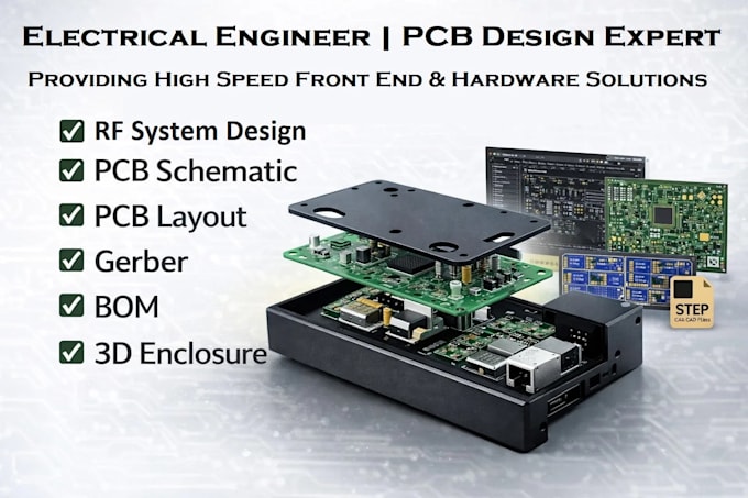
Are you looking for high-performance engineering solutions that bridge the gap between theoretical physics and real-world application? Look no further.
I specialize in the design, simulation, and optimization of RF and Electronics systems and advanced signal processing. Whether you are building a custom communication module or need to refine a complex antenna array, I provide end-to-end engineering services using industry-standard tools.
Kindly message me before placing an order to discuss your project specs or frequency requirements. Let's turn your signals into reality!
Software Expertise:
Why is simulation necessary for my RF project?
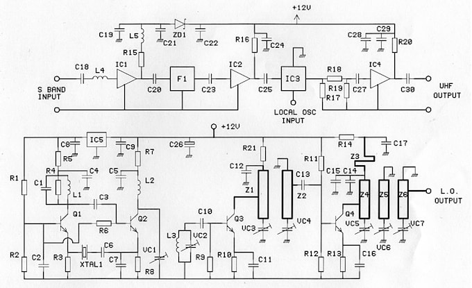
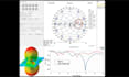
In RF engineering, "guessing" is expensive. Simulation allows us to visualize electromagnetic fields, S-parameters, and radiation patterns before a single board is manufactured. This drastically reduces the number of hardware iterations and ensures your design meets regulatory standards.
Can you fix range and connectivity issues in existing hardware?
Yes. Most range issues stem from poor antenna matching or parasitic interference on the PCB. I use 3D electromagnetic simulation to identify the root cause of signal degradation and redesign the matching network or layout to achieve peak performance.