Browse categories
Explore
Fiverr Pro
English
$
USD
Professional PCB Designer with Expertise In Embedded System and IoT Devices
HELLO THERE
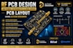
I will help you develop professional RF PCB layouts, antenna schematics, and high speed PCB solutions using Altium Designer for wireless communication and embedded electronic projects.
I'm experienced in creating clean, accurate, and manufacturing-ready PCB layouts suitable for RF systems, antenna circuits, wireless devices, IoT applications, and high frequency electronics.
WHAT I OFFER:
SOFTWARE USED:
WHAT YOU WILL RECEIVE:
WHY CHOOSE ME:
PLEASE CONTACT ME BEFORE PLACING AN ORDER TO DISCUSS YOUR PROJECT REQUIREMENTS AND COMPLEXITY.

What do you need to start the project?
Please provide your project description, circuit requirements, PCB dimensions and any reference files if available.
Do you provide manufacturing files?
Yes, I provide Gerber files ready for PCB manufacturing.
Which software do you use?
I mainly use Altium Designer for RF and high speed PCB projects.
Can you handle antenna and RF PCB projects?
Yes, I can help with RF PCB layouts, antenna schematics and wireless communication boards.
Do you provide editable source files?
Yes, source/editable project files are included based on the selected package.


