Browse categories
Explore
Fiverr Pro
English
$
USD
PCB Design and Embedded Hardware Engineer
Hi Welcome
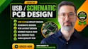
I design production ready schematics and PCB layouts for USB 2.0/3.0/3.1 hub circuits host controller ICs (GL850G, GL852G, FE1.1s, USB2517), power distribution with current limit switches, ESD/TVS protection, controlled impedance differential pair routing, and stable crystal/oscillator placement following IPC 2221 standards, built for manufacturing, not just simulation.
I also handle embedded electronics, custom controller boards, IoT devices, microcontroller boards, power and interface boards, using KiCad, Altium, EasyEDA, or Eagle. I catch what causes expensive problems later: wrong footprints, incomplete nets, poor placement, bad grounding, missing decoupling, and schematic to layout mismatches.
WHAT I DELIVER
Send me your specs or existing schematic, and let's get your board designed

Can you design USB hub circuits and USB PCBs?
Yes. I can work on USB hub and USB interface designs involving USB connectors, hub controllers, power distribution, ESD protection, decoupling, indicators, and supporting circuitry based on your project requirements.
Which PCB design software do you use?
I can work with KiCad, Altium Designer, EasyEDA, and Eagle, depending on your project and preferred source file format.
Can you select components and create footprints?
Yes. I can help identify suitable components and create or verify footprints based on manufacturer datasheets and package specifications.
Can you review my existing PCB design and fix problems?
Yes. I can review an existing schematic or PCB layout, identify issues such as incorrect connections, footprint problems, routing conflicts, clearance violations, and other design concerns, then make the required corrections.
Can you design a PCB from my circuit schematic?
Yes. I can convert your existing schematic into a professional PCB layout, including component placement, routing, design rule checking, and manufacturing ready files.
