Browse categories
English
$
USD
Connect to your AI
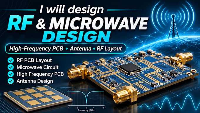
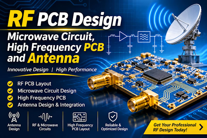
Are you looking for a reliable RF PCB layout for your wireless communication, high-frequency, or microwave circuit project?
I can help you develop a professional PCB layout with a focus on controlled impedance, signal integrity, EMI-aware routing, and antenna integration.
I specialize in RF PCB layout and electronic hardware development, helping turn circuit schematics and technical requirements into organized, manufacturable PCB designs.
What I Can Help You With
PCB Design Software
I can work with:
My goal is to understand your requirements, communicate clearly, and provide a solution tailored to your project.
Let's Discuss Your Project!
Please contact me before placing an order.
Can you design RF PCBs with controlled impedance?
Yes. I can design RF transmission lines with target impedance requirements such as 50Ω or 75Ω, based on the available PCB stackup and material specifications.
Do you provide antenna integration?
Yes. I can support antenna integration into RF PCB layouts based on your antenna design, operating frequency, and board requirements.
Can you design high frequency and microwave PCBs?
Yes. I can assist with high frequency PCB layouts, RF circuits, microwave circuits, and wireless communication boards.