Browse categories
Explore
Fiverr Pro
English
$
USD
Romania
Electronics Engineer and Modern Web Developer
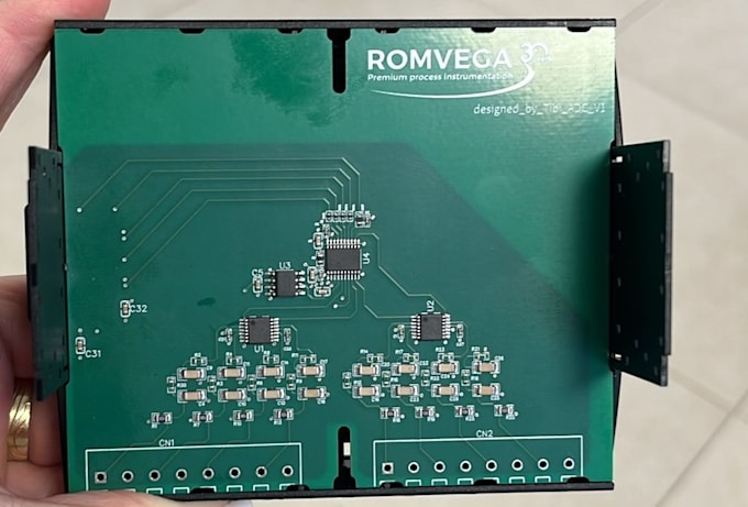
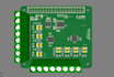
Welcome to my professional PCB Design gig!
Are you an inventor, a startup, or an engineer looking to turn your electronic circuit idea into a real, manufacturable Printed Circuit Board? You are in the right place!
I specialize in creating high-quality, reliable, and cost-effective PCB designs using KiCAD. Whether you need a simple single-layer board for a prototype or a complex multi-layer design, I am here to help.
What I offer in this gig:
What you will receive (Deliverables):
Important: Please contact me before placing an order! Every circuit is unique, and I want to make sure I fully understand your requirements so I can give you the best custom offer and delivery time.
Let's build your next awesome piece of hardware!
Specialization:
Circuit design
•
Schematics
•
Layout
•
Footprint
•
Gerber
File format:
Gerber
•
SCH
•
Software:
EasyEDA
•
KiCad
•
Other
Interface:
USB
•
SPI
•
I2C