Browse categories
Explore
Fiverr Pro
English
$
USD
Need professional RF PCB design, PCB antenna integration, RF layout, or impedance matching for your wireless product?
I can develop or optimize your RF PCB from a schematic, reference design, datasheet, or existing board for prototyping and engineering validation.
My services include:
I support wireless applications including:
RF performance depends on correct trace geometry, stack-up, grounding, return paths, via placement, antenna clearance, matching networks and enclosure constraints. I carefully consider these factors during design and review.
Let's build a reliable, manufacturable RF/wireless PCB for your product...
THANKS YOU!!!
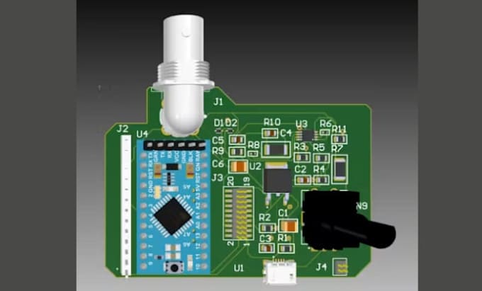
Can you design an RF PCB from my schematic?
Yes. I can review your schematic, components, RF requirements and PCB constraints before proceeding with the la
Can you design a PCB antenna?
Yes, depending on the required frequency, board dimensions, stack-up, enclosure and application requirements. Please provide the relevant technical information before ordering.
Can you work with Wi-Fi, Bluetooth, LoRa or GNSS?
Yes. RF requirements vary significantly between applications, so I recommend sending the transceiver/module part number, operating frequency and available PCB information for review.
Can you provide 50 Ω controlled-impedance routing?
Yes, when the required PCB stack-up and manufacturer parameters are available. The impedance target and transmission-line geometry should be established from the actual fabrication stack-up rather than assumed.
Can you optimize an existing RF PCB?
Yes. I can review an existing design and identify potential issues involving RF routing, grounding, impedance, antenna placement, component placement and other PCB-level factors.
Do you guarantee a specific antenna range, gain, VSWR or RF performance?
RF performance depends on many factors beyond PCB layout, including antenna construction, enclosure, materials, components, manufacturing tolerances and the final environment. I therefore do not guarantee measured RF performance without an appropriate simulation and/or measurement process.
Can you provide Gerber files?
Yes, where included in the selected package. Manufacturing outputs can be prepared according to the agreed PCB requirements.
Can you work with my existing PCB files?
Yes, provided the source files and relevant project information are available and compatible with the agreed workflow.
