Browse categories
Explore
Fiverr Pro
English
$
USD
PCB Design and Embedded Systems Engineer
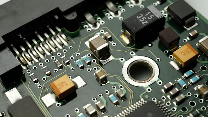
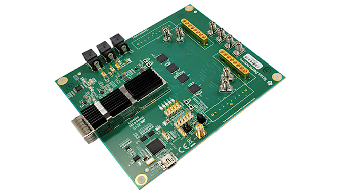
High-speed boards demand more than simple routing. I design professional RF and multilayer PCB layouts in Altium Designer with careful stack-up planning, controlled impedance, differential pairs, return paths, grounding and manufacturing compliance.
This service is suitable for USB, HDMI, LVDS, Ethernet, WiFi, Bluetooth, RF modules, mixed-signal electronics, industrial controllers and compact multilayer products.
You can receive:
The package price depends on board dimensions, layer count, pin count, routing density, interface speed and whether the schematic is already complete.
Please contact me before ordering. I will review your schematic, mechanical limits, stack-up and fabricator requirements before recommending the correct package.
Can you create the circuit schematic for this gig?
This gig mainly covers advanced PCB layout. A completed schematic should normally be supplied. Schematic review, correction or development can be purchased as an extra or included through a custom offer.
Do you perform controlled-impedance routing?
Yes. I can route according to agreed impedance targets using the selected manufacturer’s stack-up information. Final impedance accuracy also depends on the fabricator’s materials and production tolerances.
Can you route USB and HDMI interfaces?
Yes. USB, HDMI, LVDS, Ethernet and similar interfaces can be included when component specifications, interface speeds and routing constraints are supplied.
Do you provide signal-integrity simulation?
Detailed signal-integrity, power-integrity and electromagnetic simulation are not included by default. Basic engineering review or dedicated simulation can be quoted separately.
Can you design an RF antenna?
Module-level RF routing and antenna connections can be included. A fully custom antenna, matching-network optimization or electromagnetic simulation requires a separately scoped service.