Browse categories
Explore
Fiverr Pro
English
$
USD
Level 1
Has met certain performance criteria and shows strong potential in the marketplace.
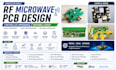
I will design professional RF and microwave PCBs optimized for signal integrity, impedance control, low noise, and reliable wireless performance.
Perfect for:
Services Offered:
I focus on minimizing signal loss, interference, noise, and routing issues for stable RF performance.
Deliverables include:
Please message before ordering for complex RF systems.

File format:
Gerber
•
STEP
Software:
Altium Designer
•
EasyEDA
•
KiCad
Interface:
HDMI
•
USB
•
Wi-Fi
•
BLE
•
BT
•
GSM/GPRS
•
LTE
•
NB-IoT
•
Ethernet
Can you design 5G and IoT RF boards?
Yes, I support RF layouts for IoT, wireless communication, and 5G applications.
Do you provide impedance-controlled routing?
Yes, controlled impedance routing is included.
Can you optimize antenna placement?
Yes, antenna matching and placement optimization are available.
Which PCB software do you use?
Altium Designer, KiCad, and EasyEDA.
Can you redesign existing RF PCBs?
Yes, optimization and redesign services are available.
Do you support multilayer RF boards?
Yes, including advanced RF stackup design.
