Browse categories
Explore
Fiverr Pro
English
$
USD
From PCB Design to WordPress, I Build What Works
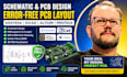
I am a professional Electronic Engineer specializing in schematic des!gn and high quality PCB layout using EasyEDA, KiCad, Altium Designer, and Proteus.
With strong hands on experience, I deliver clean, efficient, and error free PCB de-signs tailored to meet industry standards and manufacturing requirements.
Whether you are a startup, hardware developer, or based in Italy or worldwide, I ensure your project is production ready, reliable, and optimized for performance.
What I Offer:
Why Choose Me:
Let's turn your idea into a professional, manufacturable PCB design.
THANK YOU!!!


Can you work with my existing PCB files or incomplete project?
Yes, I can review, modify, and improve your existing schematic or PCB files, even if they are incomplete or need error correction.
Will my PCB design be ready for manufacturing?
I deliver fully manufacturable files including Gerber, BOM, and pick-and-place files ready for production.
Do you follow international PCB design standards?
Yes, all designs follow industry standards for reliability, signal integrity, and manufacturability to ensure high-quality results.
Can you help optimize my PCB for cost and performance?
Yes, I optimize component selection, routing, and layout to reduce cost while improving efficiency and performance.
Do you provide support after project delivery?
Yes, I offer post-delivery support to help with revisions, manufacturing questions, or any adjustments you may need.


