Browse categories
English
$
USD
Connect to your AI
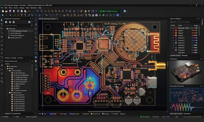
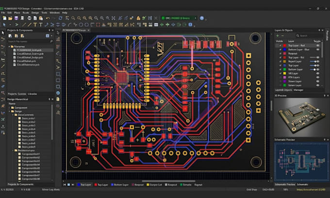
I handle KiCad schematic capture, PCB routing and custom board design for CAN bus, BMS, LoRa, BLE, USB-C, BLDC motor control, battery chargers, power supplies, mixed-signal circuits, wearables and sensor interfaces. I can also assist with PCB reverse engineering, RF layout and design-for-manufacturing (DFM) checks.
My workflow focuses on clear schematics, sensible component placement, practical trace routing, design-rule checks and organized project files. Depending on your package, you can receive:
You get a design structured for easy review, revision and handoff to your PCB manufacturer. Message me before ordering with your circuit details, board size, layer count and preferred components so I can confirm the scope, timeline and right package.
What information do you need to start my PCB design?
I need your circuit diagram, schematic, component list, board dimensions, layer requirements and any reference files. If you only have an idea, message me to discuss the project.
Can you provide manufacturing-ready PCB files?
Yes. Depending on your package, I can provide editable KiCad project files, Gerber files, drill files, BOM, 3D board views and design-rule check reports.
Can you work on specialized PCB projects like BMS, CAN Bus, LoRa and RF?
Yes, I accept specialized PCB projects involving embedded electronics, wireless communication, power management, motor controllers and sensor interfaces. Please contact me first to discuss technical requirements and project complexity.