Browse categories
Explore
Fiverr Pro
English
$
USD
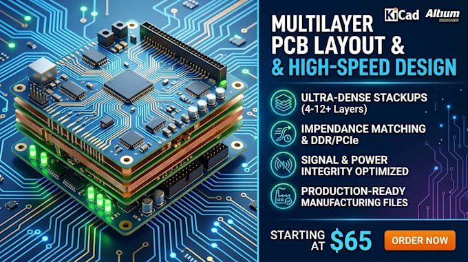
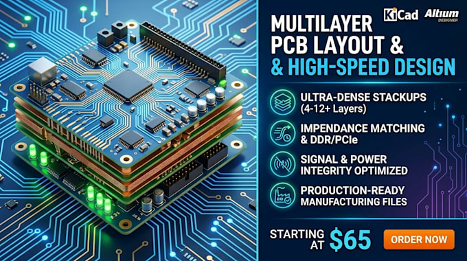
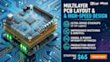
Multilayer PCB High Speed Circuit Design Expert Signal Integrity RF IoT
Struggling with crosstalk, timing jitter, or EMI failures on multi-layer PCBs?
High-speed designs require exact trace routing and stackup calculations, one mistake means an expensive re-spin.
I design high-speed, multi-layer PCBs with strict signal and power integrity, ensuring your board works reliably on the first revision.
What I Bring to Your Board:
Why Work With Me?
Don't risk a failed high-speed spin.
Send me your schematic or project details today to get started.
How do you ensure signal integrity and impedance matching for high speed signals?
I calculate custom layer stackups using track width/spacing calculators based on your fab house specs, ensuring exact 50Ω single-ended and 90/100Ω differential pair impedance.
Can you route complex interfaces like DDR memory, PCIe, or Gigabit Ethernet?
Yes. I handle high-density interconnect (HDI) routing, length/phase matching, differential pairs, and via shielding for DDR3/4, PCIe, USB 3.0, Ethernet, and RF modules.
3. What manufacturing files will I receive?
You will receive Gerber files (RS-274X or X2), NC Drill files, Pick & Place (Centroid/CPL) files, interactive BOM, 3D STEP models, and complete native source files (.PcbDoc or .kicad_pcb).
Will the PCB stackup and layout be ready for manufacturers like JLCPCB or PCBWay?
Yes. Every multi-layer board is designed against strict Design For Manufacturing (DFM) rules tailored directly to your preferred manufacturer's capability layer matrix.
What do I need to provide to start the project?
I need your circuit schematic (or block diagram), layer count requirement/preference, high-speed interface specs, and physical board dimensions or mechanical casing files.