Browse categories
Explore
Fiverr Pro
English
$
USD
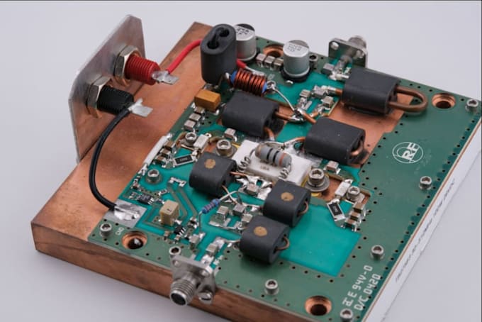
Welcome to my professional RF PCB and antenna des!gn gig.
I am Taiwo, an electronics engineer specializing in RF PCB des!gn, antenna design, multilayer PCB, high speed PCB, and CST/HFSS electromagnetic simulation.
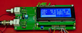
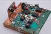
I can help you design professional and manufacturing ready PCB boards for RF, IoT, embedded systems, ESP32, Arduino, WiFi, BLE, GSM, and high-frequency applications.
My Services Include:
RF PCB Des!gn
Antenna Design
CST Simulation
HFSS Simulation
PCB Layout Des!gn
Schematic Des!gn
Multilayer PCB
High Speed PCB
Impedance Control
Signal Integrity
RF Circuit Design
Altium Designer PCB
KiCad PCB Des!gn
EasyEDA PCB
ESP32 & Arduino PCB
Gerber Files
DFM Review
Embedded Systems PCB
Software Tools:
CST Studio Suite
Ansys HFSS
Altium Designer
ADS
KiCad
EasyEDA
Why Choose Me?
Fast Delivery
Professional Communication
100% Quality Work
Manufacturing Ready Files
Affordable Price for Startups
Support After Delivery
Deliverables:
Schematic Files
PCB Layout
Gerber Files
BOM
3D PCB Des!gn
PDF Documentation
Please contact me before placing your order to discuss project requirements.

Specialization:
Circuit design
•
Schematics
•
Layout
File format:
Gerber
•
STEP
•
ODB
Software:
KiCad
•
Matlab
•
NI Multisim
•
Powersim
•
Proteus
•
Arduino
Can you review existing PCB designs?
Yes, I provide PCB review, DFM checking, and optimization.
Do you support ESP32 and IoT projects?
Yes, I design ESP32, Arduino, IoT, WiFi, BLE, and embedded systems PCB.
Can you design RF and antenna PCBs?
Yes, RF PCB and antenna design are my main specialties.
Which software do you use?
I use CST Studio, HFSS, Altium Designer, KiCad, ADS, and EasyEDA.
Do you provide Gerber files?
Yes, I provide complete manufacturing-ready Gerber files and BOM.