Browse categories
Explore
Fiverr Pro
English
$
USD
Hello There,
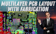
Precision and performance start with a well-engineered PCB. I design professional multilayer circuit boards that meet both functional and manufacturing standards whether for prototypes, IoT devices, or full-scale production.
With deep experience in schematic capture, PCB layout, and circuit optimization, I ensure every layer, trace, and via is clean, EMI-minimized, and DFM-ready. My workflow aligns perfectly with fabrication requirements, delivering boards that are easy to assemble and reliable in real-world conditions.
What you'll get:
Each design follows strict electrical, mechanical, and EMI/EMC standards, ensuring optimal performance and manufacturability. Whether you need a compact IoT board or a complex embedded system.
Message me to get started