I will do high speed rf pcb design microstrip layout controlled impedance kicad altium

United States

I speak English

I will design custom PCB layout fix DFM errors and convert prototypes fast

I am a dedicated electronics and custom circuit board engineer specializing in low-competition, high-demand PCB design solutions. I help hardware creators convert Arduino and ESP32 breadboard prototyp...
About this Gig

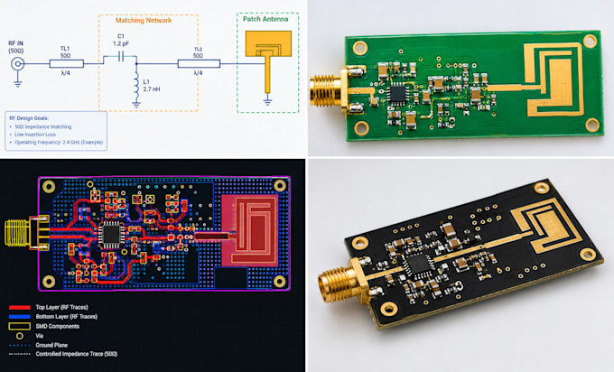
High-frequency signals, Wi-Fi antennas, and fast digital interfaces fail instantly if trace impedance is mismatched or RF routing is done incorrectly. I specialize in advanced High-Speed RF microstrip circuit design and controlled impedance stackup planning for professional wireless and high-data-rate hardware.


What I Handle in This Service:

  • Controlled impedance calculations (50Ω / 100Ω differential pairs)


  • RF microstrip and stripline routing for antennas, Bluetooth, and Wi-Fi modules


  • High-speed digital signal integrity (SPI, USB, Ethernet, DDR routing)


  • Ground plane separation and stitching via placement to eliminate EMI/EMC noise


  • Layer stackup optimization for multi-layer FR4 and high-frequency substrates


  • Full Design Rule Check (DRC) and manufacture-ready Gerber exports


  • Native source files (KiCad or Altium) with professional 3D renders


Ensure your high-frequency product passes compliance and performs flawlessly. Order now to get professional engineering for your circuit!
Specialization:

Circuit design

•

Schematics

•

Layout

•

Footprint

File format:

Gerber

•

STEP

•

BRD

•

SCH

•

PDF

Software:

Altium Designer

•

DipTrace

•

EasyEDA

•

KiCad

•

Matlab

•

Proteus

Interface:

HDMI

•

MIPI DSI/CSI

•

UART

•

USB

•

SPI

•

I2C

•

SDIO

•

PCIe

•

Wi-Fi

•

BT