Browse categories
English
$
USD
Connect to your AI
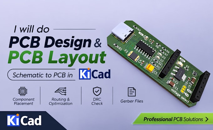
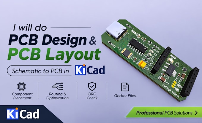
Professional PCB Designer, PCB Layout and Circuit Design
Do you have a circuit schematic that needs to be converted into a professional PCB layout?
Welcome! I'm Victor, and I specialize in PCB design, PCB layout, schematic-to-PCB conversion, component placement, and routing using KiCad.
I will help transform your existing circuit schematics into organized, reliable, and manufacturing-ready PCB layouts.
MY SERVICES INCLUDE:
TOOLS I USE
WHY CHOOSE MY SERVICES?
Whether you're an electronics engineer, student, hobbyist, or hardware developer, I'm ready to help bring your electronic project to life.
CONTACT ME BEFORE ORDERING if you have a complex project or special requirements.
Let's turn your schematic into a professional PCB!
What do you need to get started?
I need your circuit schematic, component list, preferred PCB dimensions, and any specific requirements.
Can you convert my schematic into a PCB layout?
Yes! I can convert your existing circuit schematic into a professional PCB layout with component placement and routing.
Which software do you use?
I primarily use KiCad for schematic conversion, PCB layout, component placement, and routing.
Do you support multilayer PCB layouts?
Yes, I can create 2-layer, 4-layer, and 6-layer PCB layouts depending on your project requirements.