Browse categories
Explore
Fiverr Pro
English
$
USD
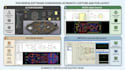
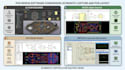
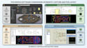
KiCad PCB Layout Expert, ESP32 S3 LoRa RF and Embedded Systems
Welcome to My Professional PCB Design Service:
A reliable Electronics Engineer for schematic design, PCB layout, and manufacturing-ready files.
I have years of experience designing high-speed, multilayer, embedded, IoT, industrial and custom electronic boards using industry-standard tools.
What I Offer:
Why Choose Me?
Contact me before placing an order to discuss your requirements and select the right package.
Which PCB software do you use?
I work with Altium Designer, KiCad, Eagle CAD, Proteus, DipTrace, EasyEDA, and PADS.
Will I receive manufacturing files?
Yes. You will receive Gerber files, BOM, NC Drill files, and fabrication-ready outputs.
Can you design multilayer PCBs?
Yes. I can design single-layer up to 16-layer PCBs with impedance control and length matching.
Can you create 3D PCB models?
Yes. I provide STEP files and realistic 3D PCB models for mechanical integration.
Do you offer PCB reverse engineering?
Yes. I can recreate schematics and PCB layouts from existing boards or reference files.


