Browse categories
Explore
Fiverr Pro
English
$
USD
PCB Design Engineer KiCad EasyEDA
Looking for a reliable PCB designer for your electronic project? You're in the right place!
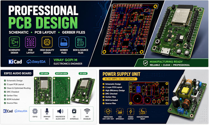
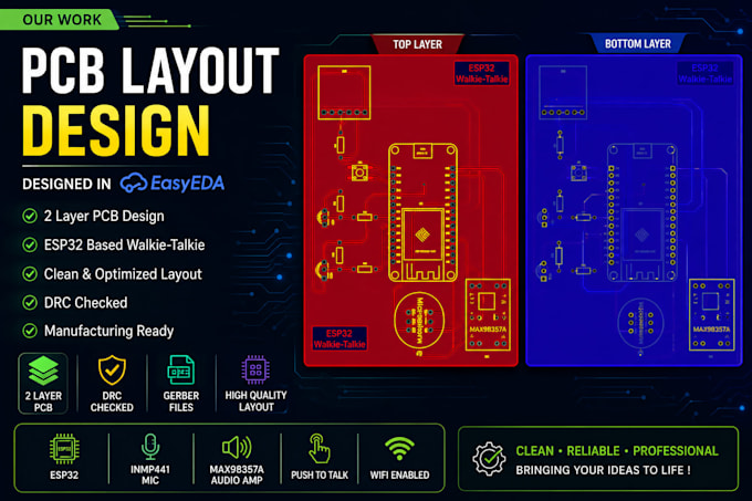
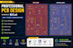
I am an Electronics and Communication Engineer specializing in PCB design using KiCad and EasyEDA. I create clean, reliable and manufacturing ready PCB layouts for prototypes, hobby projects, academic projects and custom electronic products.
What I Offer
Why Choose Me?
Before Placing an Order
Please contact me before placing an order so we can discuss your project requirements and choose the most suitable package.
I look forward to helping you bring your PCB ideas to life!
File format:
Gerber
•
BRD
•
SCH
•
Software:
EasyEDA
•
KiCad
•
Proteus
•
Arduino
Interface:
I2S
•
UART
•
USB
•
SPI
•
I2C
What do you need to start my PCB design?
Please provide your project requirements, circuit diagram or schematic (if available), component list (BOM), PCB dimensions (if required), connector details and any special design requirements. If you don't have a schematic, contact me before placing an order.
What files will I receive after the project is completed?
You will receive manufacturing ready Gerber files, PCB source files (KiCad or EasyEDA), schematic files, PDF schematic, BOM (if included) and other agreed deliverables based on your selected package.
Can you convert my hand drawn circuit or PDF into a PCB?
Yes. I can convert hand drawn circuits, PDF schematics or images into professional schematic diagrams and PCB layouts. Please contact me before placing an order so I can review your project.
Can you modify or fix an existing PCB design?
Yes. I can modify existing PCB layouts, fix design issues, update footprints, improve routing or generate new Gerber files from your existing design files.
Do you provide 3D PCB models or physical PCB prototypes?
I provide PCB design files and manufacturing ready outputs. Physical PCB fabrication, assembly, and shipping are not included in this gig unless discussed separately before placing an order.
Which PCB design software do you use?
I use KiCad and EasyEDA for schematic capture, PCB layout and Gerber generation to create professional, fabrication ready PCB designs.
Should I contact you before placing an order?
Yes. Please contact me before placing an order so we can discuss your project requirements, delivery time and select the most suitable package. This helps ensure a smooth and successful project.