Browse categories
Explore
Fiverr Pro
English
$
USD
Expert PCB Design Engineer and Multilayer PCB with Embedded Systems Specialist
Hello there!
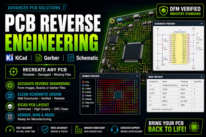
Do you need professional reverse engineering, working PCB schematic design, reliable KiCad PCB, and ready-to-use Gerber file outputs? I can help bring your PCB back to life.
I provide clean reverse engineering, tested PCB schematic design, optimized KiCad PCB layouts, and manufacturing-ready Gerber file outputs. Whether your PCB is obsolete, damaged, or missing files, I can recreate it accurately.
What You Get:
Benefits:
Efficient reverse engineering, accurate PCB schematic design, and reliable Gerber file generation save time and manufacturing cost.
Why Choose Me:
Professional KiCad PCB development, fast support, and clear communication throughout the project.


I only have a PCB image. Can you still help?
Yes! If you provide clear HD PCB images, I can perform reverse engineering and recreate the PCB schematic design.
What is reverse engineering in PCB design?
Reverse engineering means recreating the PCB schematic design and PCB layout from an existing board or Gerber file.
Do I need technical knowledge to work with you?
No, I guide clients through the process and explain everything clearly before starting the project.
Can you modify or improve my existing PCB board?
Yes, I can redesign, optimize, or improve your KiCad PCB for better performance and manufacturability.
Will my recreated PCB board work correctly?
I carefully verify every PCB schematic design and KiCad PCB layout to ensure reliability and performance.