Browse categories
Explore
Fiverr Pro
English
$
USD
PCB Designer and Embedded Systems Developer, Industrial and IoT Solutions, KiCad
You've already done the hard part the schematic is ready. Now you need a clean, manufacturable PCB layout that actually works.
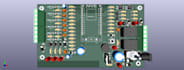
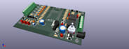
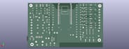
I'll take your schematic and turn it into a professional KiCad layout: proper component placement, clean routing, design rule validation, and fabrication-ready Gerber files you can send directly to any manufacturer.
What you get:
Organized component placement for signal flow and thermal management
Clean routing with proper trace widths and clearances
Full DRC validation no errors, no surprises at the manufacturer
Gerber files compatible with JLCPCB, PCBWay, and any other fab house
Fast turnaround, clear communication, and files that are ready to fabricate from day one.
Send me your schematic and let's get your board made.
File format:
Gerber
•
STEP
•
SCH
•
3DS
•
Software:
KiCad
Interface:
I2S
•
UART
•
USB
•
SPI
•
I2C
•
SDIO
•
Wi-Fi
•
BLE
•
BT
What file format should I send my schematic in?
KiCad format is preferred. I also accept PDF schematics or other formats — message me before ordering if you're unsure.
What if my schematic has errors?
If I find errors during layout I'll notify you immediately before proceeding. Schematic corrections can be added as a custom offer if needed.
Are the Gerber files compatible with any manufacturer?
Yes. All files follow standard manufacturing specs and work with JLCPCB, PCBWay, OSHPark, and any other fab house worldwide.
Can you also design the schematic from scratch?
This gig covers layout only. For full schematic capture and layout together, check my other gigs or message me for a custom offer.
What if I need more components than the package allows?
Additional components can be purchased as an extra. Message me before ordering if your design is significantly larger than the package limit.


