Browse categories
Explore
Fiverr Pro
English
$
USD
3D CAD Designer, Product Design, 3D Printing and Mold Design
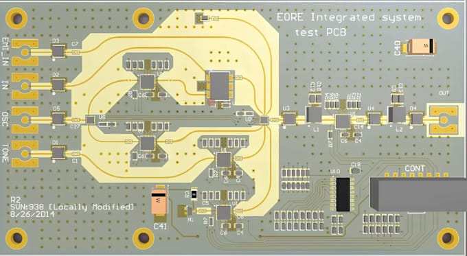
With years of experience in advanced PCB engineering, I specialize in designing high-performance RF, high-speed, multilayer, and antenna-integrated PCB systems for modern wireless and embedded applications.
Whether you are developing an IoT device, RF communication system, microwave circuit, industrial controller, or high-speed embedded hardware, I will deliver a professional production-ready PCB design optimized for performance, reliability, manufacturability, and signal integrity.
I work with industry-standard tools to create clean, accurate, and manufacturing-ready designs with exceptional attention to detail and engineering quality.
Services:
Why Choose Me
KINDLY CONTACT FIRST!
Can you help optimize an existing PCB design?
Absolutely. I can review and optimize existing PCB layouts for improved signal integrity, EMI reduction, routing quality, multilayer stackup performance, and manufacturability.
Do you provide manufacturing-ready PCB files?
Yes. All PCB designs are delivered with manufacturing-ready outputs compatible with major PCB manufacturers and assembly services.
Can you design RF, high-speed, and multilayer PCBs?
Yes. I specialize in RF PCB design, high-speed routing, controlled impedance layouts, multilayer stackup optimization, antenna integration, and signal integrity focused PCB engineering.
Which PCB design software do you use?
I primarily work with Altium Designer and also support other industry-standard tools for professional PCB layout, RF design, and multilayer PCB development.
What deliverables will I receive?
You will receive complete production-ready files including Gerber files, PCB source files, schematic files, BOM, pick-and-place files, drill files, stackup details, and 3D PCB renders depending on your package.
Do you offer schematic, layout, or Gerber file review and corrections?
Yes. I can review your PCB schematic, layout, or Gerber files and provide corrections or improvements. This includes fixing routing issues, improving signal integrity, checking design errors, optimizing stackup, and ensuring you
