Browse categories
Explore
Fiverr Pro
English
$
USD
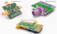
Are u looking for an experienced RF PCB engineer who can deliver manufacturing-ready microwave and antenna PCB designs? I work in RF PCB design, microwave PCB layout, antenna integration, impedance control, and EMI/EMC optimization for wireless communication systems. Using Altium Designer, KiCad, EasyEDA, Cadence OrCAD, ADS, CST, and HFSS, I create high-performance RF boards optimized for signal quality, efficiency, and manufacturability.
What I Offer
RF Applications
Deliverables
Software i use
Please contact me before placing an order to discuss your project

What information do you need to start my RF PCB project?
Please provide your project requirements, schematic (if available), PCB dimensions, target frequency, layer count, preferred components, and any RF or impedance specifications.
Can you design impedance-controlled RF and microwave PCBs?
Yes. I design RF and microwave PCBs with controlled impedance, proper stack-up planning, signal integrity optimization, and EMI/EMC considerations to ensure reliable performance.
What files will I receive after project completion?
You will receive the PCB layout files, schematic files, Gerber files, BOM, Pick and Place files, 3D PCB model, and manufacturing-ready documentation.
