Browse categories
Explore
Fiverr Pro
English
$
USD
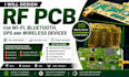
Are you struggling with poor wireless range, signal interference, antenna performance issues, or unreliable RF PCB layouts for your WiFi, Bluetooth, GPS, LoRa, or wireless device project? I can help you create a reliable, production-ready RF PCB that minimizes signal loss, improves wireless performance, and follows industry design practices.
This gig is ideal for startups, engineers, researchers, and companies developing wireless products that require RF routing, impedance control, antenna integration, and optimized PCB layouts.
What you will get:
Software:
Altium Designer, KiCad, EasyEDA, and other industry standard PCB tools.
Deliverables:
Whether you need a WiFi PCB, Bluetooth PCB, GPS PCB, RF module board, or custom wireless device, I will deliver a professional design tailored to your requirements.
Contact me before ordering to discuss your project and get the RF PCB solution

File format:
STEP
•
BRD
•
SCH
•
3DS
•
Software:
Altium Designer
•
Eagle CAD
•
KiCad
•
Matlab
•
Proteus
•
Simulink
Interface:
UART
•
USB
•
SPI
•
I2C
•
Wi-Fi
•
BLE
•
BT
•
Ethernet
What types of RF PCBs can you design?
I design RF PCBs for WiFi, Bluetooth, GPS, LoRa, IoT devices, wireless sensors, antenna circuits, and other high-frequency applications.
What files will I receive after the project is completed?
You will receive Gerber files, PCB layout files, BOM, Pick and Place files, PDF documentation, and other manufacturing-ready deliverables
Which PCB design software do you use?
I use Altium Designer, KiCad, EasyEDA, and other professional PCB design tools based on your project requirements
