Browse categories
Explore
Fiverr Pro
English
$
USD
Hardware And PCB Design Engineer
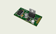
I will design a 2-layer PCB for your electronics project using KiCad.
If you already have a schematic, I can take it from there and create the PCB layout, including component placement, routing, ground planes, connectors, mounting holes, and other layout requirements.
I can work with both SMD and through-hole components and will keep the board practical to manufacture. I also check the design for common PCB layout and connectivity issues before delivering the final files.
What you will get:
If you have a specific board size, component placement requirement, connector position, or manufacturer requirement, I can take that into account while designing the board.
You can send me your schematic, circuit diagram, or project details before placing an order. I will review it and let you know what is needed for the PCB.