Browse categories
Explore
Fiverr Pro
English
$
USD
I will design professional PCB schematics and layouts using Altium Designer or KiCad.
I can help you turn your circuit idea, block diagram, reference design, or existing schematic into a fabrication-ready PCB with clean documentation.
My service can include:
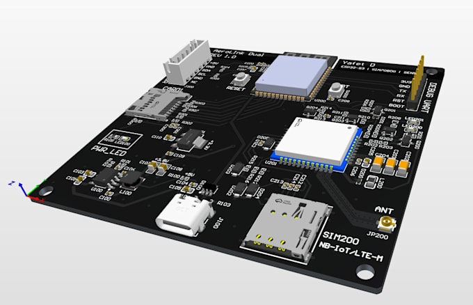
I can work on embedded, IoT, sensor, power, mixed-signal, and communication-based boards using interfaces such as UART, SPI, I2C, USB, SDIO, GSM/GPRS, LTE, BLE, Wi-Fi, CAT-M1 and NB-IoT.
I have hands-on experience designing and validating a 4-layer STM32-based wearable ECG PCB with an ADS1292R analog front end, LTE module, accelerometer, microSD storage, USB-C connection, and Li-Po power management.
Please contact me before placing an order so we can confirm the project scope, number of components, board size, layer count, required files, and delivery time.