Browse categories
Explore
Fiverr Pro
English
$
USD
TechEngineer
A few millimeters can make a real difference in RF performance.
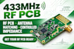
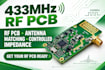
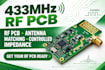
If your 433MHz project needs a clean RF layout, reliable antenna connection, and properly managed impedance, I can help turn your schematic into a practical PCB ready for fabrication.
You will receive:
What sets my work apart is attention to the RF sectionnot simply connecting components, but keeping signal paths short, organized, and fabrication-friendly.
Whether you have an existing schematic or need help refining the PCB layout, send me your files and project requirements. Lets get your 433MHz board ready for the next stage.
What do you need from me to get started?
Please provide your schematic, PCB specifications, component list, board dimensions, preferred PCB software, and antenna requirements if available.
Can you work with an existing 433MHz schematic?
Yes. I can use your existing schematic to develop the PCB layout, including RF routing, antenna matching components, and controlled-impedance considerations.
What files will I receive?
Depending on the package, deliverables can include the editable PCB source files, Gerber files, drill files, and other relevant manufacturing outputs.


