Browse categories
English
$
USD
Connect to your AI
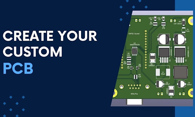
Transform your electronic idea into a 100% production-ready PCB!
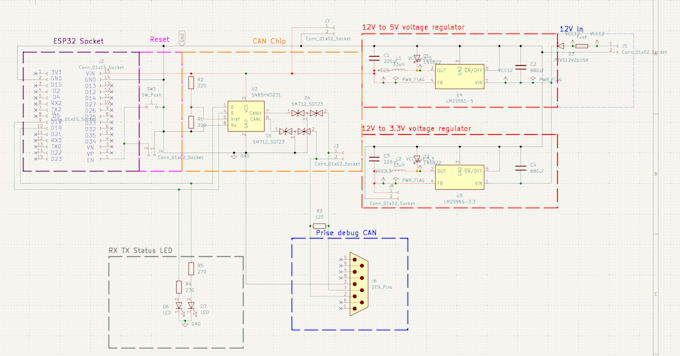
Need a custom PCB for your prototype, IoT project, or micro-controller board (ESP32, STM32, Arduino)? I provide professional schematic capture, PCB layout, and manufacturing files optimized for low-cost fabricators like JLCPCB and PCBWay.
What I offer:
Software I use: KiCad, EasyEDA, Fusion 360.
Please message me before placing an order so we can review your schematic and specs!

Specialization:
Circuit design
•
Schematics
•
Layout
•
Footprint
•
Gerber
File format:
Gerber
•
STEP
•
SCH
•
Software:
KiCad
Interface:
HDMI
•
UART
•
USB
•
Wi-Fi
•
BLE
•
BT
•
Ethernet
What deliverables will I receive upon completion?
Depending on the package chosen, you will receive complete Gerber files, the Bill of Materials (BOM), schematic diagrams, 3D STEP models, and full source files ready for manufacturing.
What software do you use for PCB design?
I primarily use EasyEDA and KiCad for schematic capture and PCB layout, ensuring professional, clean, and industry-standard source files.
Can you help with component selection and sourcing?
Yes! I optimize the design using widely available and cost-effective components (ensuring they are in stock on platforms like JLCPCB, LCSC, or DigiKey) and provide a complete BOM.
Do you offer multi-layer PCB design?
Absolutely. The Basic package supports up to 8 layers, and I can scale the layer count based on your project's technical complexity and routing requirements.